Art explaining semiconductors
The use of creative art for explaining
organic semiconductors
Nedyalka Panova (artist-in-residence) | Organic Semiconductor Centre,School of Physics & Astronomy
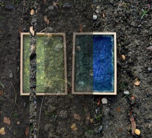
My work explores the boundaries between art and science, organic and inorganic, natural, synthetic and manmade. I work in collaboration with the Organic Semiconductor Centre led by Prof Ifor Samuel on “The use of creative art for explaining organic semiconductors”. The purpose of the project is to give a higher visibility to the interesting phenomenon of organic semiconductors using their aesthetic values.
Interdisciplinary collaboration such as this, between artists and scientists, is an increasingly popular way to bridge the gap between ‘arts and humanities’ and ‘science and technology’. It brings together experts from different fields and the outcome is art exhibitions for public domain.
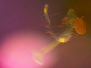
While the concept of colours and shapes of natural materials inspires artists over centuries in their studies of nature, material science progress by scientists has created a new range of synthetic materials which are manufactured using completely different set up and equipment. In this context, contemporary art and science starts asking new questions: How can art respond to the colours that are invisible to visible light? How can invisible 2D imprinted patterns be used as colours and structures? The line between the past and the future of modern technological world is drawn with a nanoscale precision and the question is: Are these new technological tools also a new media for creative endeavours?
Organic semiconductors combine properties of both metals and organic polymers with their capacity to conduct electricity. This opens new doors for applications in light communication, organic LED displays, healthcare and harvesting energy from abundant natural sources such as sun light. Their general target is to offer an alternative solution to the existing inorganic electronic components or to combine the best of both worlds in a new generation of hybrid devices.